The preparation method of the particle diffusion film is to coat the surface of the substrate with a resin layer mixed with particles (such as TiO2). The effect of light diffusion is achieved through the difference of refractive index between doped particles and film-forming resin. However, because the dispersion uniformity of particles is relatively difficult to control, the prepared product diffusion film has the disadvantages of low transmittance and small haze range.
With the development of more advanced and low-cost micro-nano fabrication technology in recent years, researchers began to explore the optimization of optical properties of diffusion films through surface microstructure. Micro-nano machining technology can be divided into three types: plane graphics technology, probe graphics technology and model graphics technology.
The core of plane graphics technology is its parallel imaging characteristics. It is characterized by the design pattern on the mask that is imaged on a flat substrate at one exposure. Optical exposure is the mainstream imaging method of planar graphic technology, that is, the so-called “lithography” method. Its biggest advantage is its high output rate. Although optical exposure is mainly used in integrated circuit manufacturing, in recent years, this process has also been widely used in micro-system technology to make a variety of micro-mechanical, micro-fluid and micro-opto-electromechanical devices. The plane process is processed in a parallel way, that is, a large number of microstructure are formed at the same time. Therefore, the plane process is a kind of process suitable for mass production.
Probe graphics technology is a point imaging method, that is, imaging is formed by point-by-point scanning. The probes here include not only solid-state probes such as scanning tunneling microprobe and atomic force microprobe but also non-solid-state probes such as focused ion beam, laser beam, atomic beam and spark discharge microprobe. However, because of the point-by-point scanning characteristic of the probe process, its imaging speed is much lower than that of the parallel imaging method in the plane process, so it is not suitable for mass production but is more suitable for micro-nano processing in scientific research.

The graphic process of the model is to copy the corresponding micro-nanostructures by using micro-nano-sized moulds. These include:
Nano-imprint technology, plastic molding technology and mold casting technology. Nano-imprinting is the use of stamps containing nano-patterns to imprint on the softened organic polymer layer, which can reproduce a large number of nano-patterns at a low cost. Nanoimprint technology has been widely used in the manufacture of organic thin-film transistors, bioelastic microstructure and so on. Molding technology is the traditional plastic molding technology, the structure size of molding is more than micron, and it is mostly used for the manufacture of microfluidic and biochips. Molding technology is also a low-cost micro-machining technology. Molding technology includes plastic casting and metal casting. Both molding and casting are the extension of traditional processing technology to the field of micro and nano. The molding speed of molding and casting is fast, so it is also a process suitable for mass production.
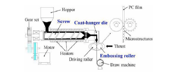
The development of the above micro-nano processing technology provides a new idea for the manufacture of surface relief light diffusion films. Some methods have been reported, such as squeeze roller imprint [25pr 46], diffusion lithography [36cr 47], hot embossing [48-50], self-assembly [39] and isotropic etching [51]. Huang of National Taiwan University and others have done a lot of research on the fabrication of light diffusion film of the cylindrical lens array, and developed the composite technology of extrusion molding and drum imprinting (shown in figures 1-4) to process the light diffusion film of the column lens array. The microstructure of the drum is copied directly to the extruded plate, and continuous production is realized. The extrusion roller imprint method uses an extruder with a die to manufacture PC and PMMA granular plates. The microstructure on the surface of the die is transferred to the surface of the prepared light diffusion film by the imprint method. the light diffusion film prepared in the experiment contains light diffuser inside and the surface has microstructure. However, the equipment required by this method is expensive, and it is still difficult to extrude with a thickness of less than 500μm diffusion film.
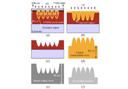
The Sung-Il Chang and Jun-Bo Yoon teams of the Department of Electrical Engineering and Computer Science of the Korea Institute of Advanced Science and Technology have done fruitful research on the fabrication of microlens arrays with high aspect ratios using diffusion lithography (shown in figure 1-5). Diffusion lithography has the ability to fabricate micro-nanostructures with a high aspect ratio which can realize bat wing radiation patterns. However, the preparation of a high aspect ratio structure by diffusion lithography requires strict control of exposure parameters and demoulding parameters.
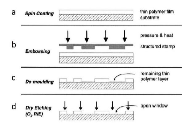
Hot embossing is a processing method in which the microstructure is prepared on the surface of the mold and then transferred to the polymer surface by imprinting. Hot embossed moulds usually use electroforming to transfer the pattern from the resist to the surface of the nickel plate [52-53]. In the hot embossing process, adjusting the temperature can improve the uniformity and depth of the transfer structure, but too high or too low temperature will affect the structure replication results. Similarly, too low pressure will lead to uneven shape and size of the microstructure; too much pressure may cause the mold and the sample to collide, thus destroying the microstructure on the mold.
